Reading Notes on Programming Massively Parallel Processors
This post contains my reading notes on the book “Programming Massively Parallel Processors: A Hands-on Approach” by David B. Kirk and Wen-mei W. Hwu.
Table of Contents
Chap4: Computing architecture and scheduling
This chapter introduces the architecture of the CUDA cores and the scheduling of the threads.
Architecture of a modern GPU
From a hardware’s perspective, a GPU is partitioned into a 2-level hierarchy of parallel processing units. The top level is the Streaming Multiprocessor (SM), which is a collection of CUDA cores. For example, the Ampere A100 GPU has 108 SMs, each with 64 CUDA cores. The bottom level is the CUDA core, which is the smallest unit of computation in a GPU.
Just like the computation units, the memory units are also grouped as a hierarchy. The global memory is the largest and slowest memory, which are shared by all the SMs. The SMs also have their own shared memory and L1 cache, which is faster than the global memory. Between the global memory and the shared memory/L1 cache, there is the L2 cache, which is shared by all the SMs. Register are the fastest memory, which is private to each thread at runtime.

Here is a table of the memory information of different memory types on NVIDIA A100 40GB GPU, you can find more details in the NVIDIA A100 datasheet:
| Memory Type | Bandwidth | Size |
|---|---|---|
| Global Memory | 1555GB/s | 40 GB |
| L2 Cache | not opened | 40 MB |
| L1 Cache | not opened | 192KB |
| Shared Memory | not opened | 164 KB |
| Register File per SM | not opened | 256KB |
| Register File per GPU | not opened | 27648KB |
Besides the bandwidth of the global memory, the bandwidth of other memory types are not opened to the public in the whitepaper, maybe you can test these numbers following here.
Block, warp, thread, and their scheduling
When a cuda kernel is called, the CUDA runtime system lanches threads that execute the kernel code. There is a 2-level abstraction of the threads: the block and the thread.
A block is the abstraction used to group threads when theses threads are lanched onto the GPU(using the <<<grid, block>>> syntax). There can be multiple blocks being assigned to the same SM at the same time, but the number of blocks that can be assigned to an SM is also limited by the hardware.
The execution between blocks is independent, which means that the threads in different blocks cannot communicate with each other and can be fully parallelized.
Within the block, programmers can synchronize threads and share data between threads, like using __syncthreads() to make sure all threads in the block have finished the previous computation before moving on to the next computation or
using the shared memory to share data between threads in the same block.
A warp is the abstraction used to group threads when the threads are getting scheduled on the SM. The warp size on most NVIDIA GPUs is 32. Threads in a block are partitioned into warps according to the thread index order. When lanching a three-dimensional grid of blocks, the threads within a block are partitioned into warps in the following order:
threadIdx.z -> threadIdx.y -> threadIdx.x
For example, for a three-dimensional 2x8x4(z, y, x) block grid, the threads are partitioned into two warps, (0, 0, 0) through (0, 7, 3) for the first warp and (1, 0, 0) through (1, 7, 3) for the second warp. Threads within a warp are executed using SIMD (Single Instruction Multiple Data) model, which means that the threads in a warp execute the same instruction at the same time. When meeting control flow divergence, the threads in the same warp between Volta architecture will be serialized, which will lead to performance degradation. From the Volta architecture on wards, the threads in different divergent paths may be executed concurrently using independent thread scheduling.
With many warps assigned to SMs and Zero-overhead scheduling, GPU can hide the latency of memory access by switching to another warp when the current warp is waiting for long-latency operations.
Resouce partitioning and occupancy
The ratio of the number of active warps to the maximum number of warps that can be active on an SM is called the occupancy. In this book, authors use many examples to show how to calculate the occupancy of an SM and how to optimize the occupancy to achieve better performance. Generally, we should take into account the following factors when improving the occupancy for a particular hardware:
- The maximum number of blocks per SM
- The maximum number of threads per SM
- The maximum number of threads per block
- The number of registers per SM/GPU
- … (shared memory size, etc.)
Querying device properties
CUDA C provides a set of functions to query the device properties, the ones that are mentioned in this chapter are:
cudaGetDeviceCount(): returns the number of CUDA-enabled devicescudaGetDeviceProperties(): returns the properties of a device, the properties include:maxThreadsPerBlock: the maximum number of threads per blockmultiProcessorCount: the number of SMsclockRate: the clock rate of the devicemaxThreadsDim: the maximum size of each dimension of a blockmaxGridSize: the maximum size of each dimension of a gridregsPerBl5ock: the number of registers per blockwarpSize: the warp size
Chap5: Memory architecture and data locality
Estimate peak performance of a kernel
At the beginning of this chapter, the authors introduce a methodology to estimate the peak performance of a kernel. Before visiting that part, we first need to know arithmetical intensity, arithmetic/computational intensity(FLOP/B) is the ratio of floating-point operations to bytes from global memory It can be a good indicator about whether the kernel is memory-bound or compute-bound. Take the matrix multiplication as an example, we read two numbers from global memory to compute 1 addtion and 1 multiplication, so the arithmetical intensity is 2/8 = 0.25 FLOP/B. Then we can obtain the peak throughput of FLOPs of this kernel by multiplying the arithmetical intensity by the peak memory bandwidth of the device, which is 1555GB/s * 0.25 = 388.75 GFLOP/s for NVIDIA A100 40GB GPU. But according to the whitepaper, the single-precision peak throughput of A100 is 19500 GFLOP/s or 156000 GFLOPS(with tensor core). This indicate that the matrix multiplication kernel is not compute-bound, which means that the kernel is not fully utilizing the peak throughput of the device.
The Roofline Model
The Roofline Model is a performance model that can help us to understand the performance of a kernel and to identify the bottleneck of the kernel.
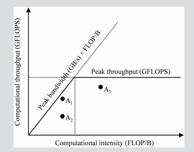
The x-axis of the Roofline Model is the arithmetical intensity, and the y-axis is the performance of the kernel. With the increasing of the arithmetical intensity, the performance of the kernel will increase until it reaches the peak throughput of the device. This divides the panel below the peak throughput into two parts: the compute-bound part and the memory-bound part. On the left of the vertical line, the kernel is memory-bound because the throughput can be increased by optimizing computational intensity, and on the right of the vertical line, the kernel is compute-bound.
From this model, we learn that we need 19500 GFLOP/s / 1555 GB/s = 12.5 FLOP/B to reach the peak throughput of the A100 GPU.
CUDA memory types
When discussing the cuda memory types, we describe different memory types from theses aspectives:
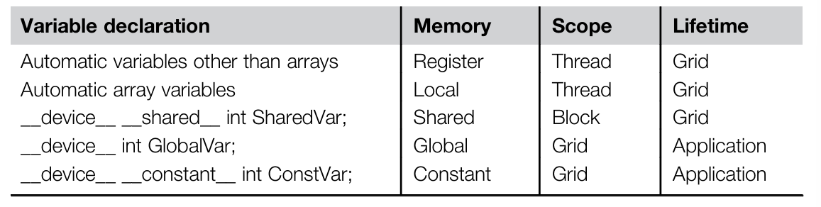
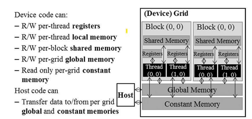
- Scope: the scope of the memory, which can be global, local, shared, constant, register. Global memory and constant memory are shared by all the threads, local memory is private to each thread (but this memory is actually from some part of global memory), shared memory is shared by threads in the same block, and register is private to each thread at runtime. Automatic variables are usually stored in registers, but if the number of registers used by a thread exceeds the limit, the variables will be stored in local memory. Automatic array variables are usually stored in local memory.
- Lifetime: the lifetime of memory, it tells the portion of the program’s execution time that the memory is valid. Global memory and constant memory are valid during the entire execution of the application, shared memory/register/local memory is valid during the execution of a grid.
- Access latency: the time it takes to access the memory, the latency of global memory is the highest, and the latency of register is the lowest. The latency of shared memory is lower than the global memory, but higher than the register. Accessing constant memory is extremely fast and parallel. There are many advantages to put operands in registers:
- it is at least 2 orders of magnitude faster than accessing global memory
- it uses fewer instructions to access the operands in the global memory
- it saves energy
- Access control: the control of the memory access, global memory and constant memory are read/write by all the threads, shared memory is read/write by threads in the same block, register is read/write by the thread that owns it, constant memory is read-only by all the threads.
- Size: we have covered the size of different memory types in the previous chapter.
- Variable declaration:
__device__: global memory__constant__: constant memory, we must declare constant variables outside the kernel function__shared__: shared memory- automatic variables: local memory / registers